zakagadir
Admin

عدد المساهمات : 3267
تاريخ التسجيل : 17/11/2007
 | | موضوع: NOR and NAND الثلاثاء يوليو 22, 2008 10:46 am | |
| IntorductionFlash memory is non-volatile computer memory that can be electrically
erased and reprogrammed. It is a technology that is primarily used in
memory cards and USB flash drives for general storage and transfer of
data between computers and other digital products. It is a specific
type of EEPROM (Electrically Erasable Programmable Read-Only Memory)
that is erased and programmed in large blocks; in early flash the
entire chip had to be erased at once. Flash memory costs far less than
byte-programmable EEPROM and therefore has become the dominant
technology wherever a significant amount of non-volatile, solid-state
storage is needed. Example applications include PDAs (personal digital
assistants), laptop computers, digital audio players, digital cameras
and mobile phones. It has also gained popularity in the game console
market, where it is often used instead of EEPROMs or battery-powered
SRAM for game save data.
Flash memory is non-volatile, which means that no power is needed to
maintain the information stored in the chip. In addition, flash memory
offers fast read access times (although not as fast as volatile DRAM
memory used for main memory in PCs) and better kinetic shock resistance
than hard disks. These characteristics explain the popularity of flash
memory in portable devices. Another feature of flash memory is that
when packaged in a "memory card," it is enormously durable, being able
to withstand intense pressure, extremes of temperature, and even
immersion in water.
Although technically a type of EEPROM, the term "EEPROM" is generally
used to refer specifically to non-flash EEPROM which is erasable in
small blocks, typically bytes. Because erase cycles are slow, the large
block sizes used in flash memory erasing give it a significant speed
advantage over old-style EEPROM when writing large amounts of data.
History
Flash memory (both NOR and NAND types) was invented by Dr. Fujio
Masuoka while working for Toshiba in 1984. According to Toshiba, the
name "flash" was suggested by Dr. Masuoka's colleague, Mr. Shoji
Ariizumi, because the erasure process of the memory contents reminded
him of a flash of a camera. Dr. Masuoka presented the invention at the
IEEE 1984 International Electron Devices Meeting (IEDM) held in San
Francisco, California. Intel saw the massive potential of the invention
and introduced the first commercial NOR type flash chip in
1988.[citation needed]
NOR-based flash has long erase and write times, but provides full
address and data buses, allowing random access to any memory location.
This makes it a suitable replacement for older ROM chips, which are
used to store program code that rarely needs to be updated, such as a
computer's BIOS or the firmware of set-top boxes. Its endurance is
10,000 to 1,000,000 erase cycles.[citation needed] NOR-based flash was
the basis of early flash-based removable media; CompactFlash was
originally based on it, though later cards moved to less expensive NAND
flash.
Toshiba announced NAND flash at ISSCC in 1989. It has faster erase and
write times, and requires a smaller chip area per cell, thus allowing
greater storage densities and lower costs per bit than NOR flash; it
also has up to ten times the endurance of NOR flash. However, the I/O
interface of NAND flash does not provide a random-access external
address bus. Rather, data must be read on a block-wise basis, with
typical block sizes of hundreds to thousands of bits. This made NAND
flash unsuitable as a drop-in replacement for program ROM since most
microprocessors and microcontrollers required byte-level random access.
In this regard NAND flash is similar to other secondary storage devices
such as hard disks and optical media, and is thus very suitable for use
in mass-storage devices such as memory cards. The first NAND-based
removable media format was SmartMedia, and many others have followed,
including MultiMediaCard, Secure Digital, Memory Stick and xD-Picture
Card. A new generation of memory card formats, including RS-MMC, miniSD
and microSD, and Intelligent Stick, feature extremely small form
factors. For example, the microSD card has an area of just over 1.5
cm², with a thickness of less than 1 mm; microSD capacities range from
64MB to 16GB, as of March 2008.
Principles of operation
Flash memory stores information in an array of memory cells made from
floating-gate transistors. In traditional single-level cell (SLC)
devices, each cell stores only one bit of information. Some newer flash
memory, known as multi-level cell (MLC) devices, can store more than
one bit per cell by choosing between multiple levels of electrical
charge to apply to the floating gates of its cells.
NOR flash
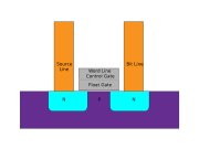
In NOR gate flash, each cell resembles a standard MOSFET, except the
transistor has two gates instead of one. On top is the control gate
(CG), as in other MOS transistors, but below this there is a floating
gate (FG) insulated all around by an oxide layer. The FG is interposed
between the CG and the MOSFET channel. Because the FG is electrically
isolated by its insulating layer, any electrons placed on it are
trapped there and, under normal conditions, will not discharge for many
years. When the FG holds a charge, it screens (partially cancels) the
electric field from the CG, which modifies the threshold voltage (VT)
of the cell. During read-out, a voltage is applied to the CG, and the
MOSFET channel will become conducting or remain insulating, depending
on the VT of the cell, which is in turn controlled by charge on the FG.
The current flow through the MOSFET channel is sensed and forms a
binary code, reproducing the stored data. In a multi-level cell device,
which stores more than one bit per cell, the amount of current flow is
sensed (rather than simply its presence or absence), in order to
determine more precisely the level of charge on the FG.
A single-level NOR flash cell in its default state is logically
equivalent to a binary "1" value, because current will flow through the
channel under application of an appropriate voltage to the control
gate. A NOR flash cell can be programmed, or set to a binary "0" value,
by the following procedure:
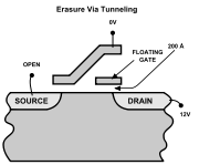
* an elevated on-voltage (typically >5 V) is applied to the CG
* the channel is now turned on, so electrons can flow from the source to the drain (assuming an NMOS transistor)
* the source-drain current is sufficiently high to cause some high
energy electrons to jump through the insulating layer onto the FG, via
a process called hot-electron injection
To erase a NOR flash cell (resetting it to the "1" state), a large
voltage of the opposite polarity is applied between the CG and drain,
pulling the electrons off the FG through quantum tunneling. Modern NOR
flash memory chips are divided into erase segments (often called blocks
or sectors). The erase operation can only be performed on a block-wise
basis; all the cells in an erase segment must be erased together.
Programming of NOR cells, however, can generally be performed one byte
or word at a time.
Despite the need for high programming and erasing voltages, virtually
all flash chips today require only a single supply voltage, and produce
the high voltages via on-chip charge pumps.
NAND flash
gate flash uses tunnel injection for writing and tunnel release for
erasing. NAND flash memory forms the core of the removable USB storage
devices known as USB flash drives, as well as most memory card formats
available today.[/b]
Block erasure
One limitation of flash memory is that although it can be read or
programmed a byte or a word at a time in a random access fashion, it
must be erased a "block" at a time. This generally sets all bits in the
block to 1. Starting with a freshly erased block, any location within
that block can be programmed. However, once a bit has been set to 0,
only by erasing the entire block can it be changed back to 1. In other
words, flash memory (specifically NOR flash) offers random-access read
and programming operations, but cannot offer arbitrary random-access
rewrite or erase operations. A location can, however, be rewritten as
long as the new value's 0 bits are a superset of the over-written
value's. For example, a nibble value may be erased to 1111, then
written as 1110. Successive writes to that nibble can change it to
1010, then 0010, and finally 0000. In practice few algorithms can take
advantage of this successive write capability and in general the entire
block is erased and rewritten at once.
Although data structures in flash memory cannot be updated in
completely general ways, this allows members to be "removed" by marking
them as invalid. This technique must be modified somewhat for
multi-level devices, where one memory cell holds more than one bit.
[b]Memory wear
Another limitation is that flash memory has a finite number of
erase-write cycles (most commercially available flash products are
guaranteed to withstand 100,000 write-erase-cycles for block 0, and no
guarantees for other blocks).[3] This effect is partially offset by
some chip firmware or file system drivers by counting the writes and
dynamically remapping the blocks in order to spread the write
operations between the sectors; this technique is called wear
levelling. Another approach is to perform write verification and
remapping to spare sectors in case of write failure, a technique called
bad block management (BBM). For portable consumer devices, these
wearout management techniques typically extend the life of the flash
memory beyond the life of the device itself, and some data loss may be
acceptable in these applications. For high reliability data storage,
however, it is not advisable to use flash memory that has been through
a large number of programming cycles. This limitation does not apply to
'read-only' applications such as thin clients and routers, which are
only programmed once or at most a few times during their lifetime.
NOR memories
Reading from NOR flash is similar to reading from random-access memory,
provided the address and data bus are mapped correctly. Because of
this, most microprocessors can use NOR flash memory as execute in place
(XIP) memory, meaning that programs stored in NOR flash can be executed
directly without the need to copy them into RAM. NOR flash chips lack
intrinsic bad block management, so when a flash block is worn out, the
software or device driver controlling the device must handle this, or
the device will cease to work reliably.
When unlocking, erasing or writing NOR memories, special commands are
written to the first page of the mapped memory. These commands are
defined by the Common Flash memory Interface (CFI) and the flash chips
can provide a list of available commands to the physical driver.
Apart from being used as random-access ROM, NOR memories can also be
used as storage devices. However, NOR flash chips typically have slow
write speeds compared with NAND flash.
NAND memories
NAND flash architecture was introduced by Toshiba in 1989. These
memories are accessed much like block devices such as hard disks or
memory cards. Each block consists of a number of pages. The pages are
typically 512 or 2,048 or 4,096 bytes in size. Associated with each
page are a few bytes (typically 12–16 bytes) that should be used for
storage of an error detection and correction checksum.
Typical block sizes include:
32 pages of 512 bytes each for a block size of 16 kiB
64 pages of 2,048 bytes each for a block size of 128 kiB
64 pages of 4,096 bytes each for a block size of 256 kiB
128 pages of 4,096 bytes each for a block size of 512 kiB
While programming is performed on a page basis, erasure can only be
performed on a block basis. Another limitation of NAND flash is data in
a block can only be written sequentially. Number of Operations(NOPs) is
the number of times the sectors can be programmed. So far this number
for MLC flash is always one whereas for SLC flash it is 4.
NAND devices also require bad block management by the device driver
software, or by a separate controller chip. SD cards, for example,
include controller circuitry to perform bad block management and wear
leveling. When a logical block is accessed by high-level software, it
is mapped to a physical block by the device driver or controller, and a
number of blocks on the flash chip are set aside for storing mapping
tables to deal with bad blocks. The overall memory capacity gradually
shrinks as more blocks are marked as bad.
The error-correcting and detecting checksum will typically correct an
error where one bit per 256 bytes (2,048 bits) is incorrect. When this
happens, the block is marked bad in a logical block allocation table,
and its undamaged contents are copied to a new block and the logical
block allocation table is altered accordingly. If more than one bit out
of 2,048 is corrupted, the contents are partly lost, i.e. it is no
longer possible to reconstruct the original contents. If this is
detected when the block is written, the contents may still be available.
Most NAND devices are shipped from the factory with some bad blocks
which are typically identified and marked according to a specified bad
block marking strategy. By allowing some bad blocks, the manufacturers
achieve far higher yields than would be possible if all blocks were
tested good. This significantly reduces NAND flash costs and only
slightly decreases the storage capacity of the parts.
The first physical block (block 0) is always guaranteed to be readable
and free from errors. Hence, all vital pointers for partitioning and
bad block management for the device must be located inside this block
(typically a pointer to the bad block tables etc). If the device is
used for booting a system, this block may contain the master boot
record.
When executing software from NAND memories, virtual memory strategies
are often used: memory contents must first be paged or copied into
memory-mapped RAM and executed there. A memory management unit (MMU) in
the system is helpful, but this can also be accomplished with overlays.
For this reason, some systems will use a combination of NOR and NAND
memories, where a smaller NOR memory is used as software ROM and a
larger NAND memory is partitioned with a file system for use as a
random access storage area. NAND is best suited to flash devices
requiring high capacity data storage. This type of flash architecture
combines higher storage space with faster erase, write, and read
capabilities over the execute in place advantage of the NOR
architecture.
عدل سابقا من قبل zakagadir في الثلاثاء يوليو 22, 2008 10:50 am عدل 1 مرات | |
|
zakagadir
Admin
عدد المساهمات : 3267
تاريخ التسجيل : 17/11/2007
| | موضوع: رد: NOR and NAND الثلاثاء يوليو 22, 2008 10:48 am | |
| Distinction between NOR and NAND flash
NOR and NAND flash differ in two important ways:
* the connections of the individual memory cells are different
* the interface provided for reading and writing the memory is
different (NOR allows random-access for reading, NAND allows only page
access)
It is important to understand that these two are linked by the design
choices made in the development of NAND flash. An important goal of
NAND flash development was to reduce the chip area required to
implement a given capacity of flash memory, and thereby to reduce cost
per bit and increase maximum chip capacity so that flash memory could
compete with magnetic storage devices like hard disks.
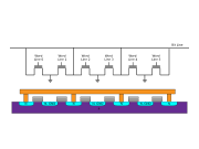
NOR and NAND flash get their names from the structure of the
interconnections between memory cells.[7] In NOR flash, cells are
connected in parallel to the bit lines, allowing cells to be read and
programmed individually. The parallel connection of cells resembles the
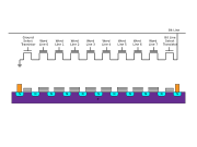
parallel connection of transistors in a CMOS NOR gate. In NAND flash,
cells are connected in series, resembling a NAND gate, and preventing
cells from being read and programmed individually: the cells connected
in series must be read in series.
When NOR flash was developed, it was envisioned as a more economical
and conveniently rewritable ROM than contemporary EPROM, EAROM, and
EEPROM memories. Thus random-access reading circuitry was necessary.
However, it was expected that NOR flash ROM would be read much more
often than written, so the write circuitry included was fairly slow and
could only erase in a block-wise fashion; random-access write circuitry
would add to the complexity and cost unnecessarily.
Because of the series connection, a large grid of NAND flash memory
cells will occupy only a small fraction of the area of equivalent NOR
cells (assuming the same CMOS process resolution, e.g. 130 nm, 90 nm,
65 nm). NAND flash's designers realized that the area of a NAND chip,
and thus the cost, could be further reduced by removing the external
address and data bus circuitry. Instead, external devices could
communicate with NAND flash via sequential-accessed command and data
registers, which would internally retrieve and output the necessary
data. This design choice made random-access of NAND flash memory
impossible, but the goal of NAND flash was to replace hard disks, not
to replace ROMs. | |
|